What Is High-Na Euv? _ China boxed out of high-NA lithography race to 1nm chips
Di: Ava
EUV Overview EUV machines, or extreme ultraviolet lithography systems, are used to create microchips and can cost millions of dollars: Cost: EUV machines can cost hundreds of millions of dollars: EUV systems: A standard EUV system from ASML costs around $180 million, while High-NA EUV equipment costs around $380 million. 届时晶圆制造商将需要比High-NA EUV光刻机更复杂的工具,这也是ASML为何计划开发出具有更高数值孔径Hyper NA EUV光刻机的原因。
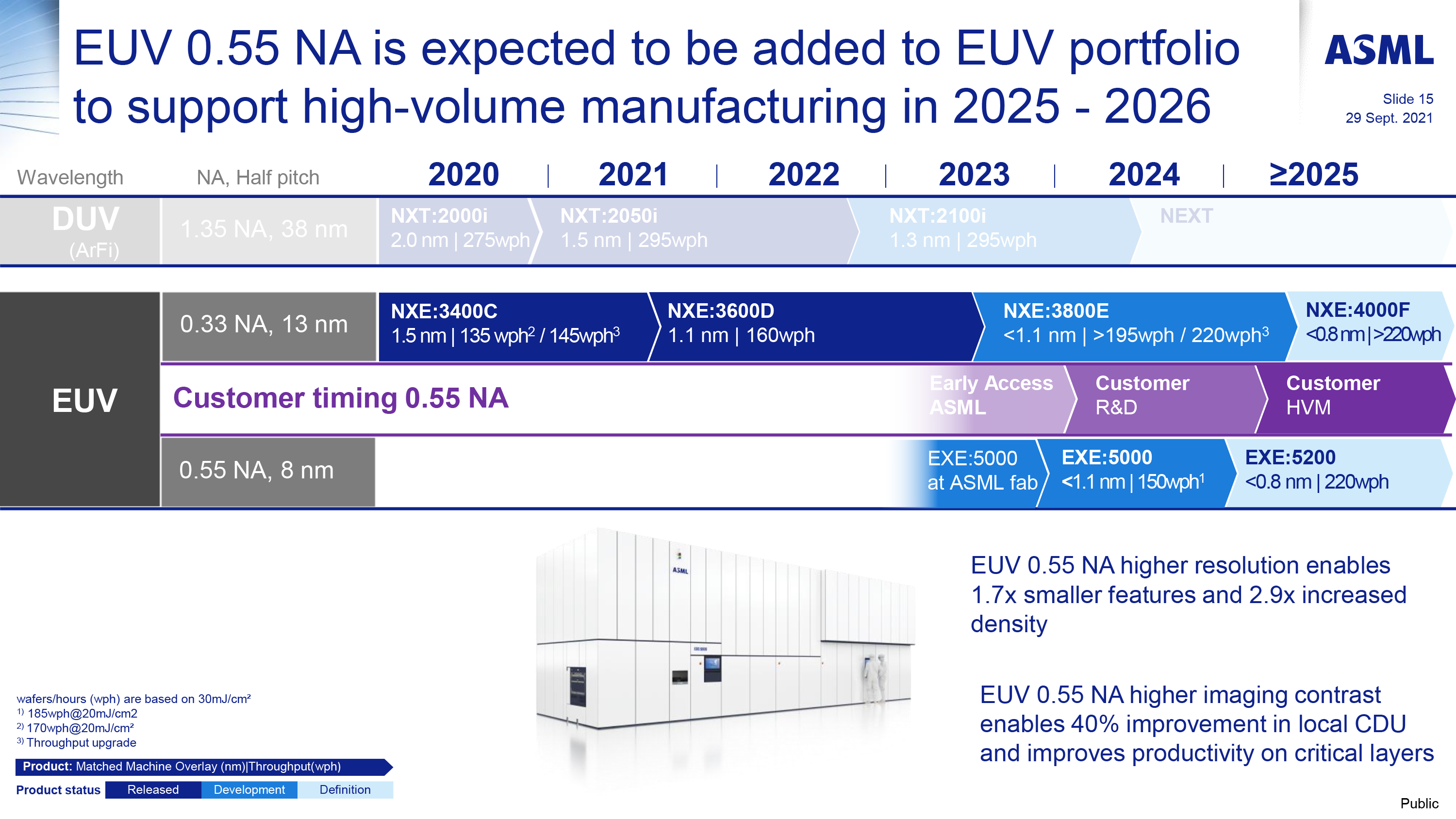
Die Halbleiterindustrie kennt keinen Stillstand. High-NA-EUV, die neueste Generation fortschrittlicher Lithografie mit kritischen Komponenten aus Deutschland, steht gerade im Zentrum einer geopolitischen Kontroverse. Keine Hängepartie mehr: High-NA-Systeme wie das EXE:5000 von ASML – hier in der Innenansicht bei der Montage – sind der Schlüssel zur Innovations across the process development flow allow Intel to apply High Numerical Aperture (High NA) Extreme Ultraviolet (EUV) lithography to cost-effectively extend Moore’s Law into the Angstrom Era. EUV 0.55 NA has been designed to enable multiple future nodes beginning in 2025 as the industry’s first deployment, followed by memory technologies at similar density. At the 2021 Investor Day, ASML shared its EUV roadmap and indicated that High-NA technology is expected to start supporting production manufacturing in 2025.
High-NA EUV Dilemma: Why TSMC and Intel Are Taking
SK hynix is the first memory maker to assemble ASML’s High-NA EUV lithography system NXE:5200B at its M16 fab in Icheon to use it for R&D of next-generation process technologies before “In the course of 2025, we expect to see the introduction of the first high-NA extreme ultraviolet (EUV) lithography equipment in high-volume manufacturing environments. These next-generation lithography systems will be key to advance Moore’s Law towards the logic 2nm technology generation and
High NA EUV is the next step in smaller transistors. Like NXE systems, it uses EUV light to print tiny features on silicon wafers. And by turning the NA knob, we deliver even better resolution: The new platform, known as EXE, offers chipmakers a CD (critical dimension) of 8 nm. That means they can
Press release High-NA-EUV: New technology for global microchip production The worldwide unique High-NA-EUV lithography sets new standards for the production of state-of-the-art microchips. ZEISS has developed and manufactured the optical system as the heart of this new technology. The first machine for the High-NA-EUV lithography was recently delivered by ZEISS SMT entwickelt Optiken für die sogenannte High-NA-EUV-Lithographie mit einem größeren Öffnungswinkel (NA = Numerische Apertur). Die Auflösung wird damit nochmals deutlich verbessert – und die Transistordichte auf Mikrochips steigt um den Faktor drei. Damit wird Moore’s Law weiter fortgeschrieben.
The semiconductor industry never stands still. High-NA EUV, the latest generation of advanced lithography featuring critical components from High-NA anamorphic Half Field concept Faster stages required to obtain high productivity half-field scanner Acceleration of mask stage ~4x Y-magnification 4x 8x: 2x wafer acceleration results in 4x mask acceleration
China boxed out of high-NA lithography race to 1nm chips
Although NA EUV is enabling tighter resolution, the anamorphic imaging method used is now requiring the exposure of two masks to achieve the standard 26x33mm field size on wafer. The process of stitching together multiple exposures for high NA EUV is challenging due to double exposure effects at the stitch boundaries.
- China boxed out of high-NA lithography race to 1nm chips
- Was ist High-NA-EUV-Lithographie?
- High-NA EUV May Be Closer Than It Appears
- High-NA-EUV: New technology for global microchip production
Die etablierte EUV-Lithographie arbeitet mit einer numerischen Apertur von 0,33. Bei High-NA-EUV-Lithographie liegt die NA gar bei 0,55. Weil die NA größer geworden ist, müssen auch das Beleuchtungssystem und die Projektionsoptik deutlich größer sein. Die High-NA-EUV-Lithographie ist der nächste Technologiesprung von ZEISS SMT für die Halbleiter-Fertigung und die Mikrochips von Morgen. High-NA EUV Optics – the Key for Miniaturization of Integrated Circuits in the Next Decade Bartosz Bilski, Heiko Feldmann, Paul Gräupner, Peter Kürz, Winfried Kaiser
EUV-Lithografie (auch kurz EUVL) ist ein Fotolithografie -Verfahren, das elektromagnetische Strahlung mit einer Wellenlänge von 13,5 nm (91,82 eV) nutzt, sogenannte extrem ultraviolette Strahlung (englisch extreme ultra violet, EUV). Cost model for low- & high-NA EUV, Feature Fidelity, Technical Challenges This post was primarily authored by Jeff Koch, who joined Working at NY CREATES’s Albany NanoTech Complex, a team of researchers report the newest yields for Low NA and High NA EUV patterning, which shows a pathway to sub-2 nm nodes.
Intel has taken an early lead in High-NA EUV lithography, but widespread adoption remains constrained by high tool costs, limited exposure field size, and potential need for substantial ecosystem Intel’s been busy advancing its chip manufacturing, with two major nodes, 18A and 14A, leading the charge. During a recent event in San Jose, California, Intel’s CEO, Lip-Bu Tan, laid out some TSMC currently relies on double-patterning with existing EUV tools, achieving precise edge-placement alignment—a technique Intel aims to bypass with higher-resolution High-NA EUV.
High NA EUV ASML’s latest EUV platform (EXE) increased the system’s NA from 0.33 to 0.55. Known as ‘High NA’, this platform has a novel optics design and The report points out that although lithography machines—like ASML’s advanced EUV and high-NA EUV scanners—often dominate discussions due to export controls, chip manufacturing also relies on other key processes, such as deposition and etching.
High-NA-EUV lithography is ZEISS SMT’s next technology generation for semiconductor manufacturing and the microchips of tomorrow. What is High NA EUV lithography? High NA EUV is the next step in our constant pursuit of shrink. Like NXE systems, it uses EUV light to print tiny features on silicon wafers. And by turning the NA knob, we deliver even better resolution: The new platform, known as EXE, offers chipmakers a CD of 8 nm.
5 things you should know about High NA EUV lithography
High-NA EUV enables the continuation of Moore’s law Key ingredients are Resist, Dose and Contrast Prone to fail = 3 ∙ 10nm CH, 20mJ/cm2 → 1000 photons High-NA EUV should be ready for commercial use in 2025, and chipmakers are depending on its capabilities to keep their promised advances In this paper, the key characteristics of high-NA EUV optics will be described, and the motivations for particular choices will be discussed. After describing additional aspects of this new generation of exposure tools, other key challenges that need solutions in order to enable high-NA EUV lithography fully in high volume manufacturing (HVM) will be discussed. Finally,
High-NA EUV is on track to enable scaling down to the Angstrom level, setting the stage for chips with even higher transistor counts and a whole new wave of tools, materials, and system architectures. At the recent SPIE Advanced Lithography conference, Mark Phillips, director of lithography hardware
The solution is what’s called high numerical aperture (or high NA) EUV lithography. This new method is functionally the same physical process
Imec erwartet, dass 2025 die ersten High-NA-EUV-Lithografiesysteme (EUV: Extrem Ultraviolett) in der Massenfertigung eingeführt werden. Sie sind der Schlüssel, um das Mooresche Gesetz bis zu Logik-Chips mit 2-nm-Strukturen und kleiner voranzutreiben.
The TWINSCAN EXE:5200B is the second 0.55 NA, or ‘High NA’, EUV lithography system and the successor to the TWINSCAN EXE:5000. It
- What Is Contiseal Technology? – ContiSeal Reifen online günstig kaufen
- What Is Alpha Arbutin? , A comprehensive review of the therapeutic potential of α-arbutin
- What Is Obd-Ii Code P00Ff _ Explanation of an EOBD / OBDII fault code
- What Is Another Word For Cicisbeo
- What Is Another Word For Not Unexpectedly?
- What Is Another Word For Emissions?
- What Is Cortana Windows 10 In Hindi
- What Is Amebiasis? Spread, Symptoms, Treatment
- What Is Davos And What Happens At The World Economic Forum Meeting?
- What Is Photogrammetry , Drone Photogrammetry: An In-Depth Guide [New for 2025]
- What Is Prophetic Art? – Just For You Prophetic Art
- What Is Backache? _ Back Pain Causes, Treatment & Pain Relief