The Benefits Of Copper Clip Over Wire Bond Packaging
Di: Ava
The introduction of improved semiconductor devices, namely wide bandgap types such as Silicon Carbide (SiC) and Gallium Nitride (GaN) will enable significantly higher performance power switching applications, especially in applications such as automotive traction inverters. SiC power semiconductor technology offers significant advantages over traditional

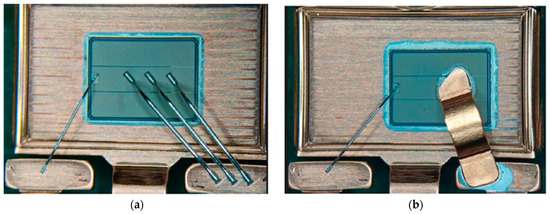
Clip-bonding technology partially replaces the standard wire-bond connection between die and lead by a solid copper bridge, which is also soldered by solder paste (Figure 1). This allows for unique package resistance, better thermal transfer, and ultra-fast switching performance due to the small package. Copper Wirebonding Copper Wirebonding refers to the wire bonding process that employs copper wires for interconnection, instead of the gold and aluminum wires traditionally used in semiconductor packaging. Copper is rapidly gaining a foothold as an interconnection material in semiconductor packaging because of its obvious advantages over gold. These advantages Figure 1. How GaN fits into the power application landscape. Image used courtesy of Nexperia How Copper Clip Packaging Improves GaN FET Performance Copper clip packaging has several advantages over wire-bond packaging, especially in higher-power applications.
Nexperia proposed CCPAK package to offer the advantages of copper clip to Power GaN FET solutions. CCPAK1212 equates to about one Wire bonding using copper or insulated wire leads to many advantages and new challenges. Research is intensively performed worldwide, leading to many new findings and solutions. This article reviews recent advances in wire bonding using copper wire or insulated wire for advanced microelectronics packaging. Journal articles, conference articles and patents
The Microelectronics Wire Bond: Past, Present and Future
a copper clip type assembly has considerably lower parasitic impedance compared to conventional power packaging at frequencies in the range of 500KHz to over 1MHz. The resistance of conventional packages recorded over this range of frequencies increases significantly as the frequency approaches 1Mhz. This is expected to be a result of skin effect
For the high-power modules packaging, Cu clip bonding has gained growing interest to replace the multiple wire-bonding for the benefits of lower resistance and improved thermal performance, which is especially beneficial for higher reliability. Interconnections on the top surface of the chip are now limiting the lifetime of power modules. It is necessary to evaluate the die top interconnection technologies in order to help module manufacturers to find a solution to prolong the lifetime of power modules. In this review, the reliability performance of different die top interconnections, such as Al bond wires, Al-clad Cu Strengthened by the innovations introduced with copper (Cu)-clip package (CCPAK) technology, Nexperia brings its long-time experience producing high-quality and robust SMD packaging to its gallium nitride FET portfolio. Based on proven technology, CCPAK provides industry-leading performance in a wire-bond–free package optimized for thermal and electrical
Nexperia’s CCPAK surface mount packaging uses Nexperia’s proven innovative copper-clip package technology to replace internal bond wires. This reduces parasitic losses, optimizes electrical and thermal performance, and improves device reliability.
Toshiba is unique amongst automotive power MOSFET suppliers in that, for the past 10 years, they have been using copper clip connectors for internal bonding in large power packages, replacing the conventional wire bonding. Since 2011 and 2015 respectively this has included the popular DPAK and D2PAK packages. This study used finite element analysis (FEA) to evaluate the electro-thermal behavior of MOSFETs with copper clip bonding, showing a significant improvement over aluminum wire bonding. The aluminum wire model reached a maximum temperature of 102.8 °C, while the copper clip reduced this to 74.6 °C.
- What is Cu clip package? copper sheet
- The Microelectronics Wire Bond: Past, Present and Future
- Copper Wire Bonding Concerns and Best Practices
- The Ideal Package Design for Silicon Carbide and Wide-Bandgap Devices
Cu clip-bonding is a promising packaging method for lower resistance, lower inductance, and higher reliability than wire-bonding. Previous studies only simply replace bond wires with Cu clips on an individual die.
The source (emitter) contact of MOSFETs (IGBTs) is one of the most sensitive joints of power semiconductor modules. Due to limitations with regards to current density and power cycling reliability, state-of-the-art aluminum wire bonding is replaced, for example, by copper wire or ribbon bonding. In this study, a novel laser micro welding technology has been implemented to Welcome to the ultimate guide to wire bonding wires. Whether you’re a newbie in the field or a seasoned professional, this comprehensive article has got you covered. In this guide, we will walk you through everything you need to know about wire bonding wires, from their basic concept to the latest advancements in the industry. Wire bonding is a critical process in semiconductor
How Copper Clip Makes Perfect Packages for the Future of Power
1.1 Copper Chip (Clip) PackageTechnology Clip Bond,It is a package process that uses copper sheet welding instead of wire bonding to connect chips and pins. Clip bond, an electrical connection that can achieve lower resistance and inductance and improve thermal performance, has been applied to power device package. Over the past few years, copper clip bonding has emerged as a promising alternative, offering superior electrical and thermal conductivity, compared to aluminum wire bonding [5].
Plasma Cleaning and Wire Bonding Wire bonding is a critical process in semiconductor device fabrication where thin wires, typically made of gold, aluminum, or copper, are used to create electrical connections between the integrated circuit (IC) or With the addition of the CFP40 and CFP60 packages, Nexperia extends the capabilities of our copper clip technology to high-power diodes
Wire bonding using copper or insulated wire leads to many advantages and new challenges. Research is intensively performed worldwide, leading to many new findings and solutions. This article reviews recent advances in wire bonding using copper wire or insulated wire for advanced microelectronics packaging. Journal articles, conference articles and patents published or Wirebonding is a commonly used method for creating interconnections between an IC on a silicon die and its packaging, in which a thin wire is connected from a bond pad on the device to a corresponding pad (i.e. lead) on the package. This connection establishes the electrical path from the internal circuits of the chip » read more Wire bonding is still the most popular chip interconnect technology in microelectronic packaging and will not be replaced by other interconnect methods for a long time in the future. Au bonding wire has been a mainstream semiconductor packaging material for many decades due to its unique chemical stability, reliable manufacturing, and operation properties.
As a key component of power electronic devices, the reliability of insulated gate bipolar transistor (IGBT) modules has attracted widespread attention. Different structural parameters of Cu clips will have different effects on the parasitic inductance, on-resistance, and junction-shell thermal resistance of IGBT modules. Therefore, firstly, the finite element models of Cu clip structures 图 (a) 引线键合和 (b) Cu Clip功率模块结构图 图 (左)铜线及(右)铜带连接工艺 Cu Clip 即铜条带,铜片。 Clip Bond 即条带键合,是采用一个焊接到焊料的固体铜桥实现芯片和引脚连接的封装工艺。 与传统的键合封装方式相比,Cu Clip 技术有以下几点优势: Wire bonds form the primary interconnections between an integrated circuit (IC) and a metal lead frame or printed circuit board (PCB) in an IC package. Wire bonding has been widely accepted in the industry for fine pitch components with high input/output (I/O) counts. This chapter introduces copper wire bonding, its advantages over gold wire bonding, and its market adoption.
Wire Bonding Process in Semiconductor Packaging
Our copper clip technology boosts power handling, electrical efficiency, and reliability – making it ideal for the incoming generation of wide-bandgap devices. Copper clip bonding, which is essential to PowerStack packaging, is a very practical implementation that is based on well established packaging capabilities and provides very low resistance on all of the current paths. Cu Clip 即铜条带,铜片。Clip Bond 即条带键合,是采用一个焊接到焊料的固体铜桥实现芯片和引脚连接的封装工艺。与传统的键合封装方式相比,Cu Clip 技术有以下几点优势:1、芯片与管脚的连接采用铜片,一定程度上取···
Combining the benefits of copper-clip packaging and wide bandgap semiconductors Nijmegen, December 11, 2023: Nexperia today announced that its GaN FET devices, featuring next-gen high-voltage GaN HEMT technology in proprietary copper-clip CCPAK surface mount packaging, are now available to designers of industrial and renewable energy Process Highlights and Capabilities Compared to traditional methods of interconnect through wire bonding, high power packages such as MOSFETs, IGBTs take advantage of copper clip technology. Copper clip attach is achieved by dispensing solder to
Cu Clip has 2 bonding methods. All copper sheet bonding method Both eviction pad and the Source pad are clip-based. This bonding technique is extra expensive and complicated, yet it can accomplish far better Rdson and much better thermal impacts. ( copper strip) Copper sheet plus wire bonding method Wire bonding using copper or insulated wire leads to many advantages and new challenges. Research is intensively performed worldwide, leading to many new findings and solutions. This article reviews recent advances in wire bonding using copper wire or insulated wire for advanced microelectronics packaging. Journal articles, conference articles and patents 安盛copper clip工艺封装,应用于功率器件封装 应用铜块连接MOS FET的Source与框架(leadframe)以获得更好的Rdson以及更好的热效应。
Types of packages based on wire bonding interconnection are leadframe packages, ball grid array (BGA) packages, and hermetic ceramic packages. As semiconductor broadens its application further, wire bonding will continue to be the major interconnection technology in high volume low cost manufacturing of semiconductor packaging industry. Conventionally, high-lead solder is employed for clip bonding due to its high thermal conductivity, good reliability, and high bonding strength.
Copper Wire Bonding Concerns and Best Practices
The cascode architecture with power gallium nitride devices uses a depletion-mode (d-mode) HEMT device and offers many advantages in higher-power–conversion applications. Improved packaging can help utilize the benefits of GaN to its fullest extent. This article details Nexperia’s development of the copper (Cu)-clip CCPAK package for its cascode
- The Best Dnd Pirate Campaign Ideas Of 2024
- The Benefits Of Roth Conversions In Retirement Planning!
- The American Finance Association
- The Best 10 Hospitals Near New Brunswick, Nj 08901
- The Best Christmas Beach Vacations For Families
- The Alix Earle Pre-Workout And Energy Drink Are Here
- The Bean Chicago Mug | Chicago: Top Sehenswürdigkeiten & Reisetipps
- The Anthropological Context Of Euskaro-Caucasian
- The Best Guns For Investors _ Are Guns Bad Investments?
- The Best Keto Chili | Hearty Texas Chili Instant Pot Recipe
- The Anatomy Of A Heart, And A Water Bottle