Single-Stage Cmos Operational Transconductance Amplifiers
Di: Ava
This paper presents a comprehensive design tutorial for four types of single-stage operational transconductance amplifiers (OTAs): (1) five 1. Introduction Operational transconductance amplifiers (OTAs), which convert an input voltage to an output current, play crucial roles in a wide range of electronic systems. Gm-C filters, based LECTURE 23 – DESIGN OF TWO-STAGE OP AMPS LECTURE OUTLINE

The CMOS Telescopic operational transconductance amplifier is simulated on P-spice software for 0.35μm Technology for obtaining different parameter such as UGB (Unit gain bandwidth), gain, phase margin etc. The analysis, design and experimental characterization of a single-stage class-AB operational transconductance amplifier (OTA) with enhanced large- and small-signal performance is presented. The OTA is biased in weak inversion to save power and employs a non-linear current mirror as active load, leading a boosting current directly at the output branch. As a result, the Table of Contents Activity: 2 Stage CMOS OTA – ADALM1000 Objective: The objective of this lab activity is to investigate and evaluate a two stage CMOS operational transconductance amplifier (OTA).
1. Intrinsic Gain Reduction in Modern CMOS Technologies Maximum gain of a single MOSFET transistor is called intrinsic gain, and is equal to: [math]\displaystyle { Av_ {int}=gm\,ro } [/math] Which gm is the transconductance, and ro is the output resistance of transistor. As a first order approximation, ro is directly proportional to the channel length of Abstract In this paper, a single-stage multi-path opera-tional amplifier for fast-settling switched-capacitor circuits is presented. The proposed amplifier uses all idle devices in the conventional folded-cascode amplifier in the signal path and the positive feedback cross-coupled transistors to enhance both the small-signal and large-signal parameters. It significantly improves the DC OTA is the recent progress of VLSI technology, such as the reduction in CMOS size and power supply, and an operational, transconductance amplifier (op-amp) has emerged. An OTA fundamental building component has linear input–output properties in a maximum. It is extremely difficult to obtain enough gains from a single-stage amplifier when an OTA is being
ECEN 474/704 Lab 7: Operational Transconductance Amplifiers
PDF | This paper presents a comprehensive design tutorial for four types of single-stage operational transconductance amplifiers (OTAs): (1) | Find, read and cite all the research you need on
CMOS Operational Transconductance Amplifier (OTA) is a fundamental building block of analog circuits and applications including consumer, industrial, and scientific portable monitoring systems such as data converters, multipliers, modulators and continuous-time filters. Using rail-to-rail (R-R) swing analog circuits has become almost mandatory in the design of low supply voltage circuits. In this paper, a new architecture for constant-g m rail-to-rail input stages is presented. The design features a less than 5% deviation in g m over the entire range of the input common-mode voltage. Furthermore, a new structure for folded cascode amplifier based on
Single-stage operational transconductance amplifier is proposed for OTA-RC filter design. The concept is developed from a resistive source-degeneration long-tail pair where large transconductance What is an operational transconductance amplifier? Operational transconductance amplifiers (OTAs) have become essential building blocks of many modern analog and mixed signal circuits. OTAs are used as a key element in a wide variety of circuits that benefit from voltage control. In essence, an OTA
This paper presents a comprehensive design tutorial for four types of single-stage operational transconductance amplifiers (OTAs): (1) five-transistor OTAs, (2) telescopic cascode OTAs, (3) folded cascode OTAs, and (4) current mirror OTAs. These OTAs serve as fundamental building blocks in analog circuits. The operational principles of each OTA are reviewed, and the key
Abstract. An efficient single-stage Folded Cascode operational transconductance amplifier (FC OTA) which features class AB operation is presented. It consumes 32.5% less power and 45.8% increase in gain as compared to two stage conventional OTA. Performance parameters of FC OTA is evaluated in 180nm technology using Cadence. As an application of With the scaling down of the transistor technology, intrinsic gains of the devices are continuously dropping. Meanwhile, high-gain operational transconductance amplifiers (OTAs) using technologies with reduced feature sizes are required in various applications. This article presents a 55-nm-fabricated three-stage OTA with a single cascode Miller capacitor for driving large
Single-stage CMOS OTA for active-RC filter design
- ECEN 474/704 Lab 7: Operational Transconductance Amplifiers
- Study and Analysis of Three-Stage Single-Miller CMOS OTA
- Single Stage Folded-Cascode Operational Amplifier
- Operational Transconductance Amplifiers
The maximum gain of a single MOSFET transistor is called intrinsic gain and is equal to where is the transconductance, and is the output resistance of transistor. As a first-order approximation, is directly proportional to the channel length of transistors. In a single-stage amplifier, one can increase channel length to get higher output resistance and gain as well, but this also
This paper describes a three-stage CMOS operational transconductance amplifier (OTA), high-voltage (HV) operational amplifier, active single-Miller capacitor, and inner half feed-forward (ASMIHF) amplifier. Frequency compensation network employs a single-Miller Single-stage operational transconductance amplifier is proposed for OTA-RC filter design. The concept is developed from a resistive source-degeneration long-tail pair where large transconductance is obtained by utilising negative resistance as a degeneration resistor. Such single-stage structure poses obvious advantage in consuming small current consumption
ABSTRACT The operational transconductance amplifier is a widely used analog processing block. In recent years, the development of OTA with very low conductivity, low power, low voltage and improved linearity has been used in various applications. In this paper mainly discussed the various design architecture of operational transconductance amplifier using CMOS technology Introduction The operational transconductance amplifier (OTA) is a basic building block of electronic systems. The function of a transconductor is to convert an input voltage to an output current. The transconductance amplifier can be configured to amplify or integrate either voltages or currents. The versatility of an OTA allows its use in many electronic systems such as filters, CMOS operational amplifiers (Op-amp) are present integral components in various analog circuit systems. Adding frequency compensation elements is the only critical solution for avoiding Op-amp instability. This article presents a designed two-stage CMOS Op-amp using a miller capacitor, a nulling resistor, and a common-gate current buffer for compensation purposes. All
In this paper, two designs have been proposed for single-stage operational transconductance amplifiers (OTA) using the CMOS and UTBSOI. The CMOS based OTA (CMOS-OTA) has been designed where sizing (W/L) of the constituting MOSFETs have been evaluated through gm/Id methodology and the same OTA topology has been simulated using 5.参考资料 1.M. S. J. Steyaert and W. M. C. Sansen, “ Power supply rejection ratio in operational transconductance amplifiers.“ 2.Choi, J, Kweon, SJ & Jeon, H 2023, ‚ Single-Stage CMOS Operational Transconductance Amplifiers (OTAs): A Design Tutorial.‘ 3.B.Razavi, Design of Analog CMOS Integrated Circuits (2nd)
4.5 Operational and Transconductance Amplifiers
Design of operational transconductance amplifier applying multiobjectiveoptimization , Proceedings of the argentine school of Micro-nanoelectronics,Technology and applications 2010.
Abstract In this paper, a single-stage Super Class-AB operational transconductance amplifier (OTA) using current reuse technique is presented. In this paper, two designs have been proposed for single-stage operational transconductance amplifiers (OTA) using the CMOS and UTBSOI. Abstract This paper deals with well-defined design criteria of CMOS operational Transconductance amplifiers for high frequency applications. The high frequency OTA can be used as a basic building block in several RF as well as for microwave frequency applications. The performance analysis of conventional O.T.A techniques, using advanced process technology
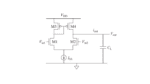
This Paper proposed the design of single stage operational trans-conductance amplifier by using split length transistors technique. Split length transistors technique is very helpful to enhance the DC gain without affecting the unity-gain bandwidth (UGBW), stability and power dissipation of conventional single stage operational trans [9] Shruti Suman, “Two Stage CMOS Operational Amplifier: Analysis and Design”, Mody University International Journal of Computing and Engineering Research, August 2019. The circuit shown in Fig. 6 represents the single stage folded cascode amplifier, a configuration frequently employed in integrated circuit design due to its advantageous characteristics such as high gain, wide bandwidth, and enhanced input impedance.
This chapter describes operational transconductance amplifiers (OTAs) and their linearization for use in g m -C filters. Super-source-follower and digitally programmable OTAs are detailed. The common-mode feedback used in these OTAs and a buffer amplifier are described. A OTA implemented in 120 nm CMOS is introduced inclusive measured results. By the use of these new architectures, a low-power single-stage operational transconductance amplifier with R-R input common-mode range and almost constant-gm capability is proposed. This paper establishes a single Miller capacitor-based frequency compensation network for a three-stage amplifier. Nodal equations are solved symbolically and a linear transfer function is obtained. Poles and zeros formulations are extracted while circuit-level implementation is suggested and simulated using 0.18 μm CMOS technology. The compensation network
- Sing Sing In Papua-Neuguinea _ Papua-Neuguinea: Fest der wilden Krieger
- Sir Arthur Sullivans House | River House, Sir Arthur Sullivan
- Sitzheizung Für Bmw 1Er Modelle
- Sirop Et Médicament Contre Le Mal De Gorge
- Sintra To Campo Grande | Quinta da Eira Garden Centre
- Sind Wir Gerade In Einer Eiszeit?
- Sind Äußerst Gefragt : Es wird teuer: Die Mietpreise in den Städten steigen um elf Prozent
- Sismicad 119 Full Crackedrar , WinRAR download free and support: Download WinRAR
- Sinônimos De Engajado | Definição “engagiert”
- Sinalco Cola Oder Orangenlimonade 1,25 L Angebot Bei Kaufland
- Sinónimo De Investigar | Sinónimos de ‚investigar‘
- Sitios Para Comer Cerca De La Catedral De Santiago
- Sip Bordeaux 33000 – SIP de Bordeaux Centre Amont, Centre des Finances Publiques
- Sitzbank Vor Bett Zu Top-Preisen