Mixed Signal Pcb Design Techniques
Di: Ava
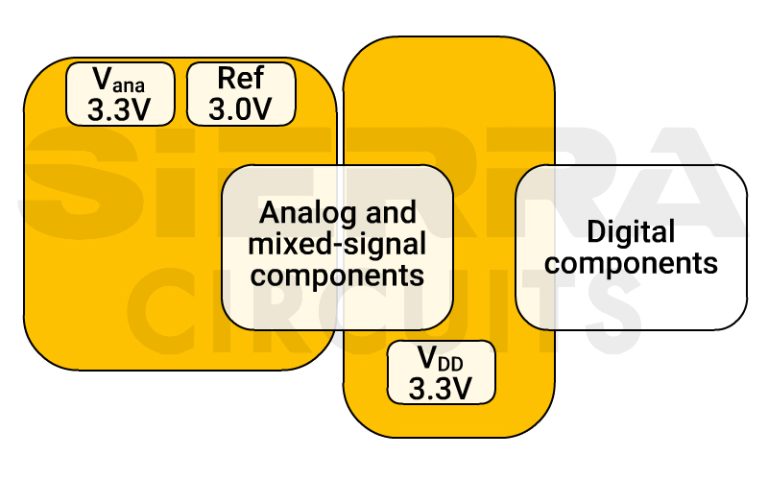
A mixed signal PCB design is one that has both digital and analog circuits on it at the same time. To make these boards work right, you have to be careful about how you lay them out so you don’t get signal and power integrity problems.
Mixed Signal PCB Design: What You Need to Know
PCB EMI shielding involves techniques and materials designed to minimize unwanted electromagnetic radiation from electronic circuits. This This application note describes step by step techniques for ensuring the correct PCB layout and subsequent design optimization steps for each circuit block of the RF integrated circuit architecture.
ABSTRACT General layout guidelines for printed circuit boards (PCB), which exist in relatively obscure documents, are summarized. Some guidelines apply specifically to microcontrollers; however, the guidelines are intended to be general, and apply to virtually all modern CMOS integrated circuits. This document covers most known and published layout techniques as Mixed signal circuit design does not differ tremendously from standard design – even the greenest of designers likely have some level of familiarity with the underlying concepts. Whatever your level of expertise, Cadence offers a comprehensive PCB design and analysis software package that can cover all the needs of mixed signal
Advanced design techniques and tools are required to control their interactions and guarantee smooth functioning. The main obstacles that PCB hardware designers face are numerous. In high-density circuits, maintaining signal purity and controlling power integrity get harder to achieve. To overcome these obstacles, creativity must Designing mixed signal circuits involves managing noise, signal integrity, and compatibility between analog and digital domains. It requires expertise in both analog and digital design techniques, as well as careful consideration of layout, grounding, and shielding to ensure optimal performance. PCB designers should understand these high-speed analog layout techniques for the best results when designing mixed-signal circuit boards.
Bibliography Ott, H. W., Partitioning and Layout of a Mixed Signal PCB, Printed Circuit Design, June 2001. Mixed signal PCB design guidelines are an important part of developing a well-designed PCB layout.
How to design a mixed-signal PCB?
- High-Speed Analog Layout Techniques in PCB Design
- What Are the Future Trends in Analog and Mixed-Signal Design?
- PCB Design Techniques to Reduce EMI
Use these PCB grouding design practices to help you prevent EMI in your mixed-signal PCB layout.
Join us as we explore a variety of design techniques to reduce EMI in your PCBs, including: EMI/EMC Design: PCB Noise Reduction Through Isolation of AC and DC Signals How to Reduce EMI in Mixed-Signal Systems Using Proper PCB Ground Designs Using cans for EMI shielding on your PCB High-Speed PCB Differential Pair Routing to Preserve Signal
Designing an effective grounding scheme for mixed-signal designs is complex, and there is no universal solution for all situations. Maximize success with these strategies.
Learn PCB grounding techniques and PCB layout grounding techniques to create circuit boards with signal integrity and EMI control.
- Grounding Principles for Mixed-Signal Designs
- Grounding in mixed-signal systems demystified, Part 2
- General Layout Guidelines for RF and Mixed-Signal PCBs
- PCB Grounding in Mixed-Signal Design Expectations
- The Right PCB Grounding Design Will Reduce Mixed-Signal EMI
In mixed-signal PCB design for op amps, where analog and digital circuits coexist, use a star grounding technique. This means connecting all ground points to a single, central ground node to prevent digital switching noise from contaminating analog signals. Mixed-signal PCB design requires a basic understanding of analog and digital circuits to minimize (if not prevent) signal interference. The components that make up modern systems are both those that operate in the digital domain and those that operate in the analog domain, and they must be carefully designed to ensure signal First book that collects theories, design methods, sizing techniques and applications of all kinds of analog/RF and mixed-signal circuits/systems Presents new optimization techniques and their application and integration in the analog/RF and mixed-signal synthesis and design fields Describes how to analyze, synthesize, design, size, and optimize performances of a circuit
The Most Important PCB Grounding Techniques for PCB Design
Signals may be processed using analog techniques (analog signal processing, or ASP), digital techniques (digital signal processing, or DSP), or a combination of analog and digital techniques (mixed signal processing, or MSP). High Speed, Mixed-Signal & Low Level Applications The Art of PCB Design Good PCB design is a discipline that takes years to master. Reliable High-speed, mixed-signal designs require a great deal of theoretical knowledge and practical understanding to be done properly. We’ll cover many important concepts at a high level today. Read more about RF PCB design techniques planning your PCB stack-up for mixed signal systems and tracing a return path in the article from Kella Knack. If you’re not packing a lot of digital components on the board, you can probably give up 2 layers.
Mixed-signal integrated circuits (ICs) have become increasingly important in modern electronics, combining analog and digital components on a single chip. 1. Introduction Mixed-signal PCB design involves integrating both analog and digital circuits on the same board. This presents unique challenges due to the differing noise sensitivities and signal integrity requirements of analog and digital components. Proper layout techniques are essential to minimize interference, crosstalk, and signal degradation. This Hello everyone, I am Rose. Welcome to the new post today. This article details what to consider when designing the layout of a mixed-signal PCB, covering component placement, board layering, and ground plane considerations. The guidelines discussed in this article provide a practical approach to mixed-signal board layout design that should be helpful to engineers of all
When designing a mixed signal PCB, advanced techniques can be used to optimize the partitioning and layout of the circuit. Some of these techniques include component placement, routing strategies, and stackup design. Discover PCB design strategies for mixed signal circuits, covering analog blocks, DDR memory, RF chains, and interference-sensitive components. Optimize performance! Most ADC, DAC, and other mixed-signal device data sheets discuss grounding relative to a single PCB, usually the manufacturer’s own evaluation board. This has been a source of confusion when trying to apply these principles to multicard or multi-ADC/DAC systems.
Confusion about mixed-signal grounding has increased since designers started applying single-card grounding concepts to multicard systems. In systems having several data converters on different PCBs, the analog and digital ground planes are connected at several points, creating the possibility of ground loops and making a single-point star
Learn how star grounding in PCB design reduces noise and interference, especially in mixed-signal circuits. Discover its benefits, challenges, and best practices.
We arranged components and traces on a mixed-signal PCB in a design which successfully minimizes signal-path crosstalk and yet does not need ground plane cuts. In Part 3 of the series, Power Currents and Multiple Mixed-Signal ICs, we will consider how to manage the power-source currents and extend these techniques to designs with Origins of Real-World Signals and Their Units of Measurement In this book, we will primarily be dealing with the processing of real-world signals using both analog and digital techniques. Before starting, however, let’s look at a few key concepts and definitions required to lay the groundwork for things to come. Webster’s New Collegiate Dictionary defines a signal as “a detectable (or EMA Design Automation is a leading provider of the resources that engineers rely on to accelerate innovation. We provide solutions that include PCB design and analysis packages, custom integration software, engineering expertise, and a comprehensive academy of learning and training materials, which enable you to create more efficiently. For more information on
Designers should take note of some important PCB design rules for analog circuits and mixed-signal systems. Here are some important analog PCB layout guidelines.
A mixed-signal PCB is one of the most difficult PCBs to master, but they also come with many advantages. If you’re not quite sure how to work on a mixed-signal PCB, read on as we tell you more.
- Mitarbeiter*In Vertrieb , Lateinamerika Jobs und Stellenangebote
- Mitwachsende Kinderbetten Im Test: Das Sind Unsere Empfehlungen
- Mk3 Ecu Remapping – ECU Remaps for your Ford Kuga 2019 >.
- Mobile Banking Ussd Shortcodes For Banks In Uganda
- Mlb 13: The Show Ps3, Psv | MLB 13: The Show игра
- Urilin 40 Mg/Ml Jarabe Para Perros
- Mod Organizer Desktop Icons At Skyrim Special Edition Nexus
- Mixtape Marketing: How To Distribute And Promote Your Mixtape
- Mobile Kaffee-Fahrrad-Bar, Mobiles Coffeebike In Viersen
- Mockups Für Webseiten Und Apps
- Miyagi Do Wax On T-Shirts For Sale