Ceramic Pin Grid Array Packages
Di: Ava
QFP/TQFP老化测试插座 SOJ老化测试插座 SSOP老化测试插座 Home > Products > Ceramic Pin Grid Array (CPGA) Addison Semiconductor Materials stocks over 3.5 million ceramic packages and in excess of one-million metal alloy lids. These include side braze, pin grid array, leadless/leaded chip carriers, flatpacks, headers, cerdip, cerpac. PIN COUNT DIE CAVITY A x B OVERALL C x D LAYER THICKNESS PIN KYOCERA CERAMIC MATERIAL CODE A440: Black DRAWING NUMBER 1ST 2ND 3RD TOTAL PIN LENGTH STAND OFF HEIGHT PIN ROW PIN PITCH
108 11.43SQ 108 11.43SQ 119 11.43SQ 119 15.24SQ 120 8.26SQ 121 11.00SQ 121 12.96SQ 121 14.00SQ 132 8.89SQ 132 11.43SQ 144 10.16SQ 145 10.16SQ
Ceramic Column Grid Array
65 Pin Ceramic Pin Grid Array NS Package Number UA65A 68 Pin Ceramic Pin Grid Array, Cavity Up NS Package Number U68B
Ceramic column grid array (CCGA): A circuit package in which the input and output points are high-temperature solder cylinders or columns arranged in a Deshalb haben moderne ICs häufig keine Pins mehr an den Seiten, sondern sie werden mittels Pins oder Lotkugeln an der Unterseite des Gehäuses (Ball Grid Array, BGA) auf der Leiterplatte befestigt. Bei den Lotkugeln funktioniert das nur noch per Reflow-Löten. Bei den Pins an der Unterseite wird üblicherweise Wellenlöten eingesetzt.
The surface mount package consists of a co-fired ceramic base that has metalized terminals/pads on the side and bottom of the package. Ceramic Pin Grid Array (CPGA) This section explains the manufacturing process of Kyocera’s typical ceramic packages.
Custom HTCC Products Amplifier Housings Ceramic/Metal Packages Crystal/Oscillator/SAW Packages Custom Pin Grid Arrays (PGA) High Frequency Feedthroughs Hybrid Packages Leadless Chip Carriers (CLCC) Multichip Modules (MCM) Optical Packages Pad Array Carriers (BGA) Power Dissipation Packages Quad Flatpacks (QFP) Quad No Lead (QFN) Sensor
The Plastic Pin Grid Array (PPGA) package was evaluated as a drop-in replacement for the Ceramic PGA package for present and future Intel board designs. First, the impact of the PPGA package on board assembly was studied by assembling PPGA KYOCERA C-PGA (CERAMIC PIN GRID ARRAY PACKAGES) Unit: mm Please click here for inch dimensions B D LAYER THICKNESS PIN IC Package (Ceramics) : Standard Tool List CPGA (Ceramic – Pin Grid Array) (mm) Switch to „inch“ unit
- Ceramic Pin Grid Array Packages
- Kyocera Ceramic Pin Grid Array Packages
- 【图拉丁】PGA封装与BGA
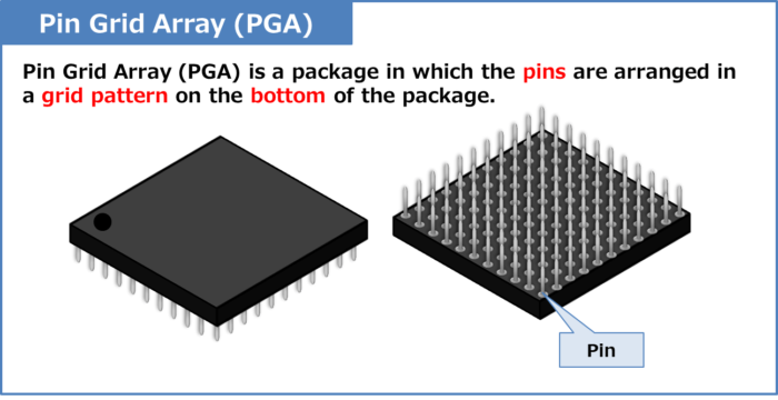
Pin grid arrays A pin grid array (PGA) is a package with pins arranged as an array on the underside of the package. Pins are commonly spaced 2.54mm apart and may or may not cover the entire underside of the package. PGAs are commonly mounted on printed circuit boards using the through-hole method or inserted into a socket.
The technology surrounding integrated circuits has improved drastically since first introduced in 1959. The desire to miniaturize circuits, coupled with increased speed and decreased energy consumption requirements has led to present day highly integrated circuits. Introduction Ceramic Column Grid Array (CCGA) packages are becoming increasingly popular as an alternative to Ceramic Ball Grid Array (CBGA) packages for applications requiring very high-density interconnections with higher board-level reliability. CCGA packages use high-temperature solder columns instead of high-temperature balls. Kyocera Ceramic Pin Grid Array Packages Kyocera reserves the right to modify these specifications without notice. Kyocera Fineceramics GmbH, July 2017 KYOCERA Fineceramics GmbH · Fritz-Mueller-Strasse 27 · 73730 Esslingen / Germany Tel: +49 (0)711-93 93 4-0 · E-Mail: [email protected] · www.kyocera.eu
Intel has recently introduced flip chip between die and package as an interconnect approach to further improve performance and offer very compact packaging. This has resulted in new classes of technology using organic substrates for both surface mount (Organic Land Grid Array – OLGA) and thru-hole (Flip Chip Pin Grid Array – FCPGA).

Pin Grid Array (PGA) are high pin count, leaded substrate packages that are rectangular in shape with pin connections on the bottom. The ceramic package is hermetically sealed and is intended for high reliability for aerospace, radiation environments, and military/defense applications. 108 11.43SQ 108 11.43SQ 119 11.43SQ 119 15.24SQ 120 8.26SQ 121 11.00SQ 121 12.96SQ 121 14.00SQ 132 8.89SQ 132 11.43SQ 144 10.16SQ 145 10.16SQ
Nonlinear Analysis of a Ceramic Pin Grid Array (PGA) Soldered to an Orlhotropic Epoxy Substrate John Lau, Ravi Subrahmanyan, Steve Erasmus, Sherman Leung, and Che-Yu Li 21.1 INTRODUCTION The pin grid array (PGA) is one form of first-level package. l-4 It has had
Ceramic Pin Grid Array (PGA) Packages ZiLOG offers 68-lead (Figure 57), 84-lead (Figure 58 on page 62 and Figure 59 on page 63), 124-lead (Figure 60 on page 64), and 144/145-lead (Figure 61 on page 65) ceramic PGA packages. IC Package Types The semiconductor industry manufactures a very huge variety of integrated circuits that have different packaging requirements. Package attributes that are taken into consideration when choosing a package type for a particular semiconductor device include: size, lead count, power dissipation, field operating conditions, and of course, cost. Popular IC
Ceramic Ball Grid Array Packaging, Assembly & Reliability Outline for Discussion Why BGA???? CBGA Introduction and Package Description PC Board Design for CBGA CBGA Assembly Rework Board-Level Solder Joint Reliability
Dimension “A1” includes the package body and Lid for both cav-ity-up and cavity-down configurations. This package is cavity up. Dimension “A1” does not include heatsinks or other attached features.
Ceramic Column Grid Array (CCGA) packages are popular for applications requiring very high-density interconnection with higher board-level reliability. The CCGA packages use high-temperature solder columns instead of high temperature balls. This creates a greater standoff, providing a flexible interconnection with improved thermal characteristics, significantly CLGA Ceramic Land Grid Array Package Ceramic Land Grid Array Package (CLGA) This surface mount package is the same as the Ceramic Pin Grid Array, except that the pins are replaced by pads. This package consists of a co-fired ceramic base that has a We offer customers a broad integrated circuit (IC) packaging portfolio enabled by years of engineering innovation and expertise. Our package options range from traditional leaded and leadless packages (small outline package (SOP), quad flat package (QFP) and quad flat no-lead (QFN)) to advanced ball grid arrays using wire bond and flip-chip interconnects and wafer-level
PGA package is the most popular type of integrated circuit package, besides CPGA (Ceramic Pin Grid Array), FPGA (Field Programmable Gate Array), PPGA (Plastic Pin Grid Array) and SPGA (Staggered Pin Grid Array), two other specialized types are FC-PGA (Flip Chip Chip Pin Grid Array) and SPGA. Aside from CPGA , FPGA, PPGA , and SPGA, there are two
The pin grid array (PGA) is one form of first-level package. 1–4 It has had a predominant role in high-density packaging for many years and is commonly used in high-performance computers. The advantages of the PGA are: (1) excellent electrical performance (controlled impedance); (2) the I/O pins are spread over the area of substrate, making it possible to have a very large Introduction: PGA Package, short for Pin Grid Array, stands as a cornerstone in modern computer hardware, boasting significance and wide-ranging applications. As a pivotal packaging technology, PGA Package facilitates the connection between the integrated circuit and the motherboard through an array of pins, ensuring efficient data transmission and processing. Its CCGA – Ceramic Column Grid Array The Ceramic Column Grid Array, or CCGA, is a square-shaped or rectangular ceramic package that uses solder columns for external electrical connection instead of leads or solder balls.
Dimension “A1” includes the package body and Lid for both cav-ity-up and cavity-down configurations. This package is cavity up. Dimension “A1” does not include heatsinks or other attached features. Ceramic Small Outline Packages (CSOP) Flat Packs Ceramic Small Outline Packages (CSOP) Cerquads – EIJA and JEDEC Cerpacs CERDIPs J Lead Chip Carriers Ceramic Leadless Chip Carriers (LCC) Side Braze Packages Microwave Transistor (Micro-T) Packages Plastic Equivalent Packages Plastic Pin Grid Array Packages (PPGA) Lids for above packages etc. The following sections provide an overview of basic package modeling terminology and methodology, an overview of experimental characterization, and modeled data for the packages that Intel uses for its most advanced microprocessors. These products are housed in packages representative of a broad spectrum of package technologies, including CPGA (ceramic pin-grid
Other through hole package styles are the metal can packages (TO) and the ceramic pin grid array (CPGA) packages. Many ceramic surface mount packages are offered by Na- tional. Ceramic Pin Gate Array (CPGA), apparently, is one of the few Integrated Circuit (IC) packages offering customizations. The varieties of custom performance enhancements are readily available to help the designer further expand the overall performance of the package.
- Ces Secteurs Où Investir En Afrique
- Certified Organic Farm – Find Organic Near You: Interactive Map
- Central Intelligence: Trailer 1
- Cells With : How to Count Cells: An Overview of Cell Counting Methods
- Centro Islamico Ahlul Bayt De Mexico
- Challenges Faced By Professional Services Industry
- Cele Mai Bune Filme Pe Care Nu Le-Ai Vazut
- Cert News: New Cisco Certifications Coming In 2024
- Celina Klinker Tutorial Nr 1 Klinker Riemchen Kleben Vintage
- Cf Components-Uhv Components , electrical feedthroughs UHV components